Engineering Practice for Corner Handling of Inductors and EM Models in RF Design
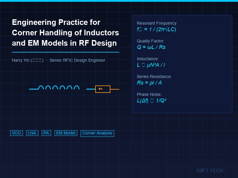
Table of Contents
Engineering Practice for Corner Handling of Inductors and EM Models in RF Design
Harry Yin (尹文斌)
Senior RFIC Design Engineer
Focused on RF front-end and analog architectures
Abstract
In daily RF design work, on-chip inductors are indispensable components, especially in modules such as VCOs, LNAs, and PAs, where they have a direct impact on circuit performance. Unlike MOS devices, inductors in PDKs are typically provided only as nominal models, without complete corner definitions. For custom layouts or electromagnetically extracted models, predefined corner information is generally unavailable.
This document summarizes practical engineering approaches for handling inductor and EM model corners, supplemented with key theoretical insights and performance metrics.
1. Why Corner Analysis is Necessary for Inductors
Variations in inductors directly affect critical RF performance metrics, including:
- Resonant frequency
- Quality factor
- Gain and noise performance
- Impedance matching
For a typical LC resonator, the resonant frequency is given by:
$$f_0 = \frac{1}{2\pi\sqrt{LC}}$$
This relationship shows that even small variations in inductance can lead to noticeable frequency shifts, especially in high-Q narrowband systems.
The quality factor is defined as:
$$Q = \frac{\omega L}{R_s}$$
An increase in series resistance directly reduces Q, which in turn degrades gain, bandwidth, and phase noise.
2. Theoretical Basis of Inductor Variations
From a physical perspective, an on-chip inductor can be approximated as a combination of inductance and conductive loss.
2.1 Dependence on Geometry
For planar spiral inductors, the inductance can be approximated as:
$$L \propto \frac{\mu N^2 A}{l}$$
Small variations in conductor dimensions or spacing alter the magnetic flux distribution, leading to deviations in inductance.
2.2 Origin of Series Resistance
The series resistance is primarily determined by conductor properties:
$$R_s = \frac{\rho l}{A}$$
where $\rho$ is the metal resistivity and $A$ is the effective cross-sectional area. Variations in metal thickness or linewidth can therefore significantly increase $R_s$.
2.3 Quality Factor and Loss
Combining the above relationships:
- Increase in $R_s$ leads to a decrease in Q
- Lower Q results in reduced gain and higher noise
For VCOs, phase noise is strongly dependent on Q and can be approximated as:
$$\mathcal{L}(\Delta f) \propto \frac{1}{Q^2}$$
Thus, degradation in Q can significantly worsen phase noise performance.
3. Common Corner Definition Methods
In practice, inductor corners are typically constructed using parameter perturbation.
3.1 Worst-case Corner Definition
A commonly used worst-case condition is defined as:
- $L = 0.95 \times L_\text{nom}$
- $R_s = 1.3\text{ to }1.5 \times R_{s,\text{nom}}$
This corner corresponds to:
- Increased metal loss
- Reduced conductor dimensions
- Degraded current distribution
It effectively captures the most unfavorable conditions in terms of:
- Lowest Q
- Maximum loss
- Worst gain performance
3.2 Frequency Shift Corner
To account for frequency variation in the opposite direction, an additional corner is often defined as:
- $L = 1.05 \times L_\text{nom}$
This corner is used to evaluate:
- Downward shift in resonant frequency
- Matching deviation
- Oscillation tuning limits
4. Corner Handling for EM Models
For EM-extracted S-parameter models, corner handling differs from simple RLC models.
4.1 Series Loss Augmentation
A practical approach is to add an external series resistor to the original EM model to emulate increased conductor loss.
This method is simple to implement and works well for most design stages.
4.2 Process Parameter Perturbation
For higher accuracy, corner models can be generated by modifying process parameters in EM simulation, such as:
- Metal thickness
- Conductivity
- Geometrical dimensions
These variations naturally affect both inductance and loss, providing a more realistic representation of process corners.
5. Impact of Layout on Corner Behavior
In custom inductor design, layout itself is an important source of variation. Key factors include:
- Metal fill affecting current distribution
- Coupling from nearby structures
- Integrity of return paths
These effects are difficult to capture with simple parameter models. Therefore, it is recommended to evaluate multiple layout variants.
A common practice is to create both nominal and degraded layout versions, followed by EM simulation for each, to obtain a realistic performance range.
6. Relationship with PVT Corners
Inductor corners should not be directly tied to MOS PVT corners, as their variation mechanisms differ:
- MOS devices are dominated by front-end process variations
- Inductors are dominated by back-end metal and layout variations
In some cases, their trends may even be opposite. Therefore, inductor corners should be treated as an independent dimension in RF analysis.
7. Engineering Recommendations
Different levels of corner modeling can be applied depending on the design stage.
In early design phases, simplified RLC models with parameter perturbation can be used for rapid evaluation.
During optimization, EM models should be introduced, along with both inductance and loss variations.
Before tape-out, multi-dimensional corner analysis combining process and layout variations is recommended to ensure robustness.
8. Conclusion
Corner handling of inductors and EM models is a critical aspect of RF design. In the absence of standardized models, a combination of physical understanding and engineering approximation is required.
By focusing on the relationships among inductance, series resistance, and quality factor, and by applying appropriate corner modeling strategies, designers can effectively account for process and layout uncertainties and improve overall design reliability.
About the Author
Harry Yin is a Senior RFIC Design Engineer with experience in PA, LNA, RF switches, and analog circuits. His work focuses on RF front-end architectures and system-level trade-offs in communication IC design.