An Introduction to RF Switches: When Analog Intuition Stops Working
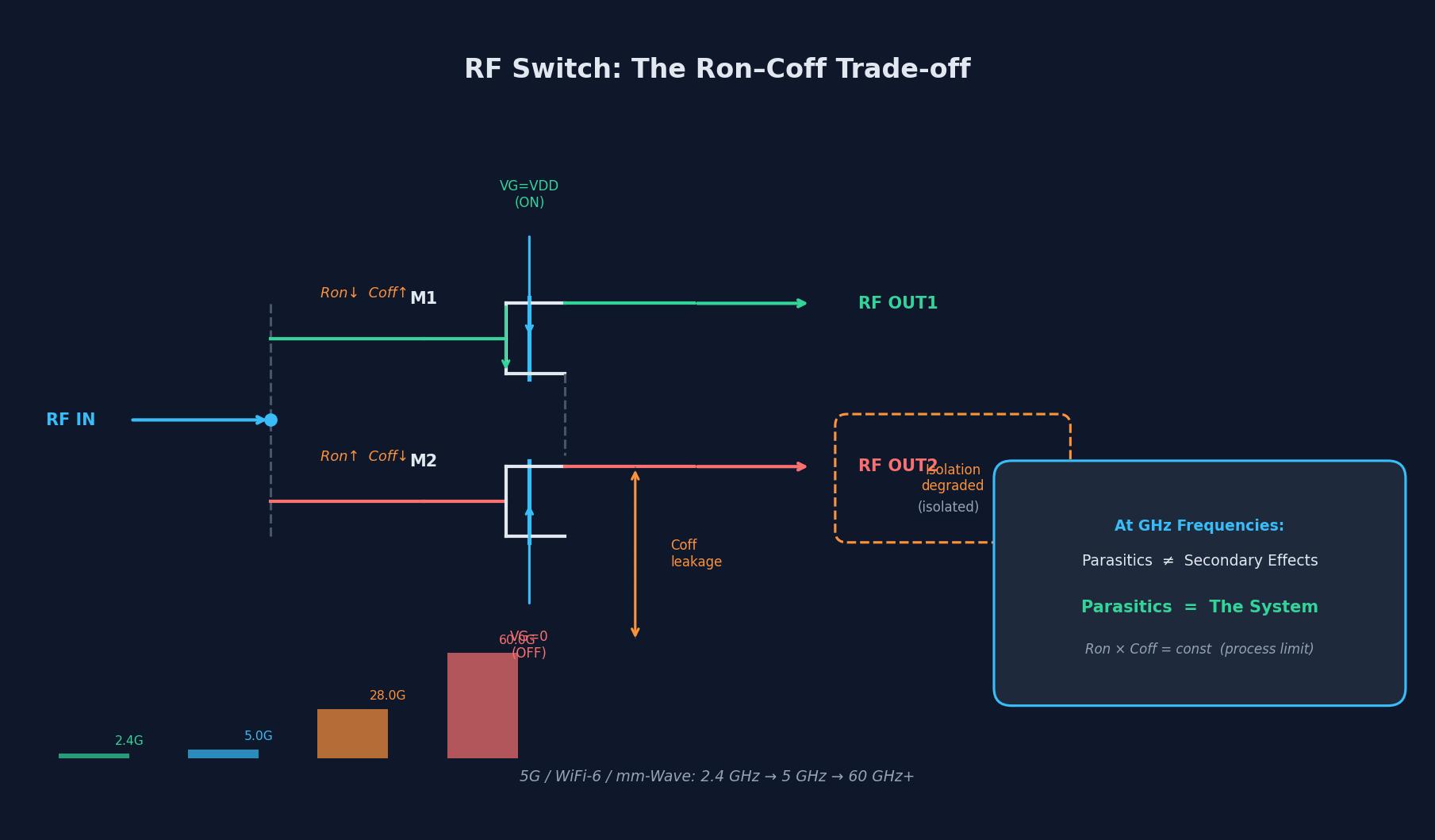
Table of Contents
An Introduction to RF Switches: When Analog Intuition Stops Working
Harry Yin (尹文斌)
Senior RFIC Design Engineer
Focused on RF front-end and analog architectures
Overview
For many analog IC engineers, the first encounter with an RF switch often feels like a complete collapse of intuition.
It is still a MOS transistor. It is still fundamentally a “switch.” Yet once the operating frequency moves from MHz into the GHz world, many of the design instincts built in analog design suddenly stop working. Techniques that once felt natural and reliable may now become the very reason performance degrades.
This transition is one of the most important turning points for engineers moving from analog IC design into RFIC design.
1. The Fundamental Challenge: MOS Is Never an Ideal Switch
In low-frequency analog circuits, we are used to treating a MOS transistor as a controlled resistor. When turned on, it behaves like Ron; when turned off, it is treated almost like an open circuit. The design objectives are straightforward: reduce on-resistance, improve speed, minimize charge injection, and lower leakage current. In many cases, simply increasing the MOS size improves performance because a wider device reduces Ron.
But the RF world introduces a brutal reality:
A MOS transistor is never an ideal switch.
Once frequency enters the GHz range, all the parasitic components that were previously ignored begin to dominate circuit behavior. Even when a MOS transistor is turned off, parasitic capacitances such as Cgs, Cgd, and Cds still exist. At low frequencies, these capacitances appear nearly open because their impedance remains large. But at 2.4 GHz, 5 GHz, or even millimeter-wave frequencies, those same capacitances become real leakage paths for RF energy.
This is often the moment when engineers first realize that an RF switch is never truly “OFF.”
And this is precisely where RF design fundamentally separates itself from traditional analog design.
2. The Ron–Coff Trade-off: The Most Fundamental Constraint
In analog switch design, making the MOS device larger is usually considered beneficial because larger width reduces Ron. In RF switch design, however, increasing device size also increases parasitic capacitance. Ron improves, but Coff increases at the same time, leading to degraded isolation, increased RF leakage, and poorer impedance matching.
This creates one of the most fundamental trade-offs in RF switch design:
Lowering Ron requires a larger MOS device, which in turn increases Coff.
In practice, the product Ron × Coff is largely determined by the process technology itself — it is a figure of merit that engineers cannot fundamentally overcome by clever circuit design alone. This is a completely different engineering philosophy from low-frequency analog design. Many optimization methods that once worked in a single direction now become multidimensional compromises.
- Improving insertion loss may hurt isolation
- Increasing power handling may worsen Ron
- Enhancing linearity may significantly increase parasitics and chip area
This is where many engineers begin to truly understand the difficulty of RF design.
3. A New Engineering Mindset: From Voltages to Waves
The deeper transformation is not only about device behavior. It is about changing the way engineers think about circuits themselves.
Low-frequency analog design is largely a world of voltages and currents. Engineers focus on gain, bandwidth, noise, and stability. RF design, however, becomes a world of waves. Signals are no longer simply voltage variations — they become electromagnetic energy propagating and reflecting through transmission structures.
As a result, the language of design changes completely.
Instead of gain and phase margin, engineers begin discussing S11, S21, return loss, and isolation. Instead of asking whether a function works correctly, the question becomes whether energy is transferred correctly.
For many engineers entering RF for the first time, this shift can feel deeply uncomfortable. Because suddenly, even a “wire” is no longer just a wire.
4. Layout Is Part of the Circuit
In low-frequency analog design, layout is mostly considered a physical implementation of the schematic. In RF design, layout itself becomes part of the circuit. A short metal interconnect may already introduce noticeable inductance. A small routing change may alter impedance matching. Even the placement of a via can affect system isolation.
This is why RF engineers often experience a painful but important moment in their careers: schematic simulations look excellent, yet performance collapses after layout extraction.
And this is also why many experienced RF designers say:
“RF design is ultimately a battle against parasitics.”
The real challenge is often not the schematic itself, but electromagnetic simulation, parasitic extraction, and layout co-design. Because at GHz frequencies, engineers are no longer designing ideal circuits. They are designing within a physical world filled with coupling, reflections, and parasitic interactions.
5. Why RF Switches Are a Perfect First Lesson
RF switches happen to be one of the clearest examples of this transformation.
At first glance, an RF switch appears to be a simple component. But behind it lies a complex interaction between impedance matching, parasitic modeling, wave propagation, linearity, power handling, and system-level trade-offs. For many engineers, moving from analog switches to RF switches is not simply a change in operating frequency — it is a complete upgrade in engineering mindset.
Because at this point, engineers begin to truly understand something fundamental about high-frequency design:
In the RF world, parasitics are not secondary effects.
Parasitics are the system itself.
About the Author
Harry Yin is a Senior RFIC Design Engineer with experience in PA, LNA, RF switches, and analog circuits. His work focuses on RF front-end architectures and system-level trade-offs in communication IC design.